What's new

The latest news is that China's 7nm chips are manufactured using synchrotron radiation, which has 40 times the capacity of EUV lithography.

Why not continue discussing CCP?

How many times do I need to say it?

The EUV/DUV sold by AMSL to China cannot produce 7nm chips!!!

Only Huawei has the technology to produce chips without using ASML products!

Can you understand human language?
You are an idiot. I am putting you an ignore.

It is well documented that SMIC has produced the 7 nm chips using multiple rounds of patterning using DUV technology. TSMC used the same process before the advent or EUV, but the yield is very poor and the cost of the chip using this process could be 10x the cost using EUV.

The DUV machines being used by SMIC are most likely either from ASML or Nikon.
You are a hopeless little idiot.

Return to a common sense question. If you use ASML/Nikon to produce chips, Americans won't know????

I have enough evidence. If you use ASML to produce 7nm chips. Americans will immediately remotely shut down all EUV/DUVs!

Finally. Make you despair.

Screenshot_20230918_145130.jpg
:rofl: :rofl: :rofl: :rofl: :rofl:
 
China VS the world.

Geely produces 7nm chips.


Huawei produces cars.


The original plan is use 7nm chip in 2022.

But because of USA sanctions, it was delayed up to the end of 2023.
 

Huawei Kirin 9000S

Let’s jump right in with the talk of the town, Huawei’s Kirin 9000S produced by SMIC. The chip uses a custom Armv9 core, and a custom GPU architecture designed by Huawei. The ability to design leading architecture in China is a big deal. While the US has stopped AMD and Intel from various CPU deals with China in the past, it has not done been able to do so with Arm. Partially this is due to the joint venture Arm has in China, which is not under their direct control. Another reason is that the Armv9 instruction set is from Arm Cambridge. Additionally, they utilize Arm’s licensed A510 cores. The A510 core is designed in Arm’s Sophia France R&D center + Cambridge.

The chip is technically incredible. The performance and power consumption profile in a variety of tests bring it on par with 1 to 2-year-old Qualcomm chips (S888 & S8G1). The RF side of the chip is amazing, using an integrated modem that is on par with Qualcomm’s current best. This is not surprising given Huawei was a bit ahead of Qualcomm before they were banned from using TSMC. The most important point is that the RF Front End chips are also domestically produced, which was a capability many thought China lacked.

The most shocking finding is that when direct comparisons are done on identical IP, the Arm A510 for Huawei’s Kirin 9000S built on SMIC’s N+2 (7nm) and 2022 Qualcomm’s S8G1 built on Samsung’s 4LPX process. The performance and power consumption of the Arm A510 cores are effectively on par with each other despite the process technology gap, indicating SMIC N+2 is better than most in the west realize. Part of the reason these chips are so close to each other is Samsung’s poor yield and SMIC’s good yield.

Put simply, Kirin 9000S is a better designed chip than the West realizes. It has solid power and performance. Even with the lackluster export controls, this is a leading edge chip that would be near the front of the pack in 2021, yet was done with no access to EUV, no access to cutting edge US IP, and intentionally hampered. We cannot overstate how scary this is.


SMIC N+2, A True 7nm, Good Yields


The process is a true 7nm process in terms of density. While the engineering decisions on specific pitches are different from TSMC’s 2018 7nm, it should be considered a similar process technology, and SMIC is at worst only a handful years behind TSMC. One could argue that SMIC is at most only a few years behind Intel and Samsung despite restrictions. As SMIC is replicating what has been done elsewhere, the gap could be even narrower due to their excellent engineering pool from mainland China as well as many courted immigrants from Taiwan that were formerly employed by TSMC.

As mentioned earlier it is on par with Samsung’s 4LPX in performance and power. The big questions are yield and volume. While some pundits claim the yield is only 10%, we don’t believe that. In fact, we believe that SMIC’s process has good yield. There’s no definitive number here, but there are some data points that indicate this.

Why? We’ve heard a few soft remarks from our sources in China that yield is good. Allegedly their D0 is currently about ~0.14. For reference, TSMC’s N5 and N6 nodes are about half that. TSMC of course is the gold standard, and Samsung/Intel “7nm” are closer although still ahead of what SMIC has achieved. Yield being this decent already is a huge flag that the SMIC N+2 process technology is healthy and developing. Parametric yield is the more important, unknown metric. But hearsay isn’t enough on its own.

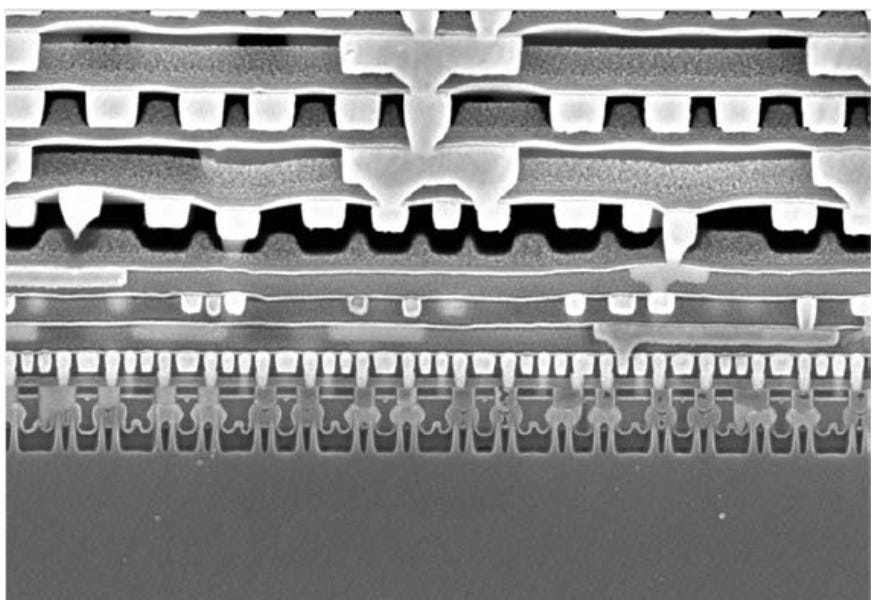
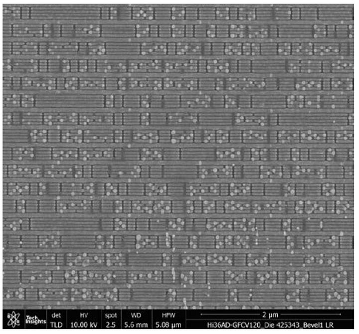
For more tangible evidence, the channels, gates, and drains on the FinFETs as well as the contacts and lower metal layers look fairly clean. A process with low yield probably won't look as uniform. See these images from the TechInsights public brief. We recommend looking at their full teardown for more images and the exact pitches.


https%3A%2F%2Fsubstack-post-media.s3.amazonaws.com%2Fpublic%2Fimages%2F9e0ec77c-a3a4-429a-9aed-6ccc59ca13d9_738x687.png


The last reason is related to the apparent binning of the chip. "Binning" in semiconductor manufacturing refers to the process of sorting and categorizing integrated circuits (like CPUs or GPUs) based on their performance and quality after they have been manufactured and tested. While chips can have defective transistors, called catastrophic yield, in many cases, working transistors still fail various performance and power tests. This is known as parametric yield. If a process technology has low parametric yield, the firm managing yield for the chip can make the binning process less stringent to improve the parametric yield. More chips can pass various tests, but it also leads to higher variability.

This has been done with mobile chips that yielded poorly in the past, for example the Qualcomm S8G1 on Samsung’s 4LPX. In the case of the S8G1, different devices with the same chip would have differences upwards of 10% on fully heat soaked devices in the same environmental conditions. While we haven’t seen rigorous testing of many devices in the same environment, there is enough on various Chinese forums to show that device to device variation is quite low.

None of this is bullet proof, but we believe that SMIC has good yield, and the 10% yield number some pundits have said is nonsense to downplay the significance. This is a real high volume production process technology. Just like Apple is the guinea pig for TSMC process nodes and helps them ramp and achieve high yield, Huawei will likewise help SMIC in the same way.

As a reminder, Huawei released the first TSMC N5 produced chip, so this is a role they are very capable of playing. In two years, SMIC will likely be able to produce large monolithic dies for AI and networking applications. This is a similar time scale to what Broadcom and Nvidia’s transition to new process technologies.

......


Continuing above article.

Btw, I just know how the processor was made.

It explains why my Intel Core i7 benchmark result is not the same as someone's posted online. I thought my Windows, motherboard, RAM, etc are the causes. It turns out the same Core i7 will have different results, because of yield factor (failure in production). If one processor turns out to be well produced, it will have higher performance (less defects). And no processor is the same because of defection.

The same smartphone can have different benchmark results, even thou all of them are brand new, tested right away out of the box.
 
Last edited:

5nm Is Possible


ASML is ramping to ship over 400 ArFi tools a year, with claims of hitting 600 DUV tool capacity by 2025. More than half of the capacity is penned for demand they see coming from Chinese fabs. While these tools will be distributed widely, to many companies, SMIC is the largest individual customer for ASML in China.

ASML openly says this is explicitly for over 1.5 million excess/inefficient wafers per month by 2030, with an additional 150k WPM of excess/inefficient capacity added each year. ASML says this is due to regionalization of semiconductor supply chains, but that’s just a cover for China achieving semiconductor independence and using DUV to reach 5nm.

To be abundantly clear, it is explicitly built into ASML’s capacity plans and forecasts that China will be semiconductor independent from a semiconductor fabrication standpoint as per their last investor day. The rest of the supply chain is of course still highly intertwined including equipment, consumables, and design IP.

A “5nm” process that achieves over 130 million transistors per mm^2 is possible to achieve with high yields using ArFi multi-patterning. The overlay capabilities of the 1980i series is good enough that 5nm can be manufactured at acceptable yields.

This SMIC N+3 “5nm” process would also be economical to produce given the level of governmental subsidies. While the lack of EUV would increase total lithography costs by 55% to 60% in our estimation, remember that lithography is only ~30% of the total process cost at 5nm currently. This means that the total process cost would only be ~20% higher versus a 5nm that utilizes EUV. Yield likely takes a hit and therefore the actual number will be higher due to more defective chips per wafer, but it will not be an insurmountable barrier for China.

If nothing changes with current restrictions, we expect Huawei and SMIC to have a true 5nm based chip in 2025 or 2026 with large scale AI chips not so long after. The current export controls are not limiting China’s manufacturing capabilities or capacity.

....

Yes, China is able to produce 5nm chips using DUV in 2025-2026.

But the cost will be 20% more expensive compared with using EUV.
 
Last edited:
The news comes from a product launch on 12 September 2023 reported by Huawei. Huawei mentions that they work with the Beijing Synchrotron Radiation Facility, BSF, on chips. Then the Chinese media enquired about its two factories in Xiongan and Shanghai, owned by CGST and Zhangjiang Hi-Tech, that can manufacture 7nm chips via synchrotron radiation.

The Beijing Synchrotron Radiation Facility, BSF, and Tsinghua University have collaborated to propose the SSMB-EUV light source solution (Steady State Microbeam), which overturns the concept of traditional lithography technology by no longer relying on shrinking the light source to improve the quality of the image, but rather, by enlarging and elongating the light source, to achieve the automatic adjustment of the different wavelengths of light, so as to achieve a higher degree of precision.

Of course, all the news now comes from the unofficial media splicing bits and pieces together and making guesses. It has not been confirmed by official organisations such as Huawei or Tsinghua University. I can understand if people don't believe it.


Satellite view of SSMB-EUV light source factory:
View attachment 953685

In June 2021, the official Chinese government media reported on the completion of the construction of the SSMB-EUV light source factory:
View attachment 953686

In February 2023, a press release from Tsinghua University's official media stated that the university's SSMB-EUV light source solution and technology had been put to practical use after spending 10 years and had solved a problem that was a major national need in the field of photolithography:
View attachment 953687

I think this project is not related to the current Huawei 7nm chips.

I think this project is aiming for 1nm chips in the future.

There are still several years away for the launching of 1nm chips, there are still a lot of time for China.

I also wonder, what is China progress on the carbon or graphene based chip?
 
You are an idiot. I am putting you an ignore.

It is well documented that SMIC has produced the 7 nm chips using multiple rounds of patterning using DUV technology. TSMC used the same process before the advent or EUV, but the yield is very poor and the cost of the chip using this process could be 10x the cost using EUV.

The DUV machines being used by SMIC are most likely either from ASML or Nikon.
You need to chill bro. Nobody knows which process was used and nobody even knows it was a loss as you said. Nobody is stupid enough to make 40mil phones for a loss. If it is indeed SMIC, Mr. Liang the Chinese from Taiwan aka Taiwanese found a way to scale it up and improve the yield.

There is news coming out that SMIC Duvs can't satisfy 40mil chips and SSA800 is already running and producing. It's up to you to believe what you want but just because India can't make it doesn't mean we can't. Chandrayaan 2 failed to land and Chandrayaan 3 needed US deep space support. China can only depend on ourselves and we made it the first time. You see the gap between us? We don't just talk we take action
 
You need to chill bro. Nobody knows which process was used and nobody even knows it was a loss as you said.
No one knows for sure because neither SMIC nor Huawei has spoken about it, but there is plenty of circumstantial evidence that DUV process with multiple patterning was used. Some idiotic Chinese posters are claiming that China produced an indigenous EUV machine and it was used to produce the chips.

Nobody is stupid enough to make 40mil phones for a loss. If it is indeed SMIC, Mr. Liang the Chinese from Taiwan aka Taiwanese found a way to scale it up and improve the yield.

There is news coming out that SMIC Duvs can't satisfy 40mil chips and SSA800 is already running and producing.
Is SSA 800 a 7nm EUV lithography machine ? Can you please provide its technical specs are provide details of how many have been sold with the dates and the buyers or at least provide the date on which it was first delivered to SMIC ?
It's up to you to believe what you want but just because India can't make it doesn't mean we can't. Chandrayaan 2 failed to land and Chandrayaan 3 needed US deep space support. China can only depend on ourselves and we made it the first time. You see the gap between us? We don't just talk we take action
How is any of this relevant to this thread ? If you want to discuss these topics please start your own thread instead of derailing this one. I will ignore anyone who persists in making irrelevant posts.
 
No one knows for sure because neither SMIC nor Huawei has spoken about it, but there is plenty of circumstantial evidence that DUV process with multiple patterning was used. Some idiotic Chinese posters are claiming that China produced an indigenous EUV machine and it was used to produce the chips.
That's the point isn't it? You don't know, i don't know. So what are we discussing here about something nobody knows. We know for a fact, the 2nm table was completed, the optica were completed, and the source was tested. Do you know we have a EUv source since 2017,it was even published in CAS website, but it is at 32nm.
Is SSA 800 a 7nm EUV lithography machine ? Can you please provide its technical specs are provide details of how many have been sold with the dates and the buyers or at least provide the date on which it was first delivered to SMIC ?
Nobody knows. But we do know it was already produced and tested. You just have to wait okay.

How is any of this relevant to this thread ? If you want to discuss these topics please start your own thread instead of derailing this one. I will ignore anyone who persists in making irrelevant posts.
The point is you benchmark yourself to India. A few years ago nobody believed China could make advanced turbofans. We tend to be discreet and let the results speak for itself.

very impressive design from huawei
Wow so nice of you mole. Lol
 
I think this project is not related to the current Huawei 7nm chips.

I think this project is aiming for 1nm chips in the future.

There are still several years away for the launching of 1nm chips, there are still a lot of time for China.

I also wonder, what is China progress on the carbon or graphene based chip?
Or some kind of glass based chips?
 
Nobody knows. But we do know it was already produced and tested. You just have to wait okay.
Is it some state secret that nobody knows ? The information in the public domain is that SSA 800 is a 28 nm machine and it will be delivered by the end of 2023 ? So, please tell me do you think it is plausible that some Chinese company fabricated a 7 nm chip using an indigenous EUV lithography machine like some Chinese idiots are claiming?
The point is you benchmark yourself to India.
I don't, but I see that you do. This thread is about whether China produced the 7nm chip used in Huawei's phone using an indigenous machine or not. Do you have an opinion on that except saying " No one knows" - when in fact even the well- informed Chinese know that not even the code name for an indigenously built Chinese EUV lithography machine exists .
 
We are not talking about t-shirts and towels here.

The reason that I am asking about costs is that the chips could have been made using new tech in an experimental setting- which could be prohibitively expensive in a commerical setting. For example, you can "manufacture " gold in a particle accelerator, but the cost is prohibitive.
No we are talking about solar panels and other electronics costs

Ultimately China will figure out how to decrease the cost

They always do
 

Back
Top Bottom