beijingwalker
ELITE MEMBER

- Joined
- Nov 4, 2011
- Messages
- 65,187
- Reaction score
- -55
- Country

- Location
China plans to build a giant chip factory driven by particle accelerator
- Scientists said this unprecedented technology can overstep US sanctions and make China a new leader in semiconductor chip industry
- Plans are now in progress to construct a huge particle accelerator to help researchers put into practice the cutting-edge technology
Published: 9:00am, 25 Sep, 2023
Cutting-edge technology to manufacture microchips could give the Chinese semiconductor industry a way around US sanctions.
China is exploring new avenues to bypass restrictions on lithography machines, which are used in the production of microchips. Using particle accelerators to create a novel laser source, researchers are laying the foundation for the future of semiconductor fabrication.
Plans are now under way to construct a particle accelerator with a circumference between 100-150 metres (328-492 feet) – roughly the size of two basketball courts. The accelerator’s electron beam will transform into a high-quality light source for on-site chip manufacturing and scientific inquiry.
The team from Tsinghua University is in active discussions with authorities in Xiongan New Area to select a construction site for the cutting-edge project.
Contrary to commercial players such as Advanced Semiconductor Materials Lithography (ASML), which favours reducing the size of chip-making machines for export, the Chinese project aims to localise manufacturing by building a colossal factory housing multiple lithography machines around a single accelerator.
This innovation could foster high-volume, low-cost chip manufacturing and potentially propel China into a leadership role in the industrial production of advanced chips, known as 2nm (nanometre) chips, and beyond.
Lithography systems are among the most sophisticated pieces of machinery ever created by humans. Currently, extreme ultraviolet (EUV) with ultra-short wavelength is widely used in the production of chips with 7nm nodes and below.
ASML is the only company that owns the technology and therefore dominates the market. As of the end of 2022, ASML had delivered 180 EUV systems. It also plans to ship 60 EUVs this year, according to a Bloomberg report published in April.
While there are many researchers chasing the technology, the Chinese scientists have been exploring a different path. It is a project that has been running since 2017, but due to Huawei’s breakthroughs in chip manufacturing, it was recently catapulted into public view.
“One of the potential applications of our research is as a light source for future EUV lithography machines. I think this is why the international community is paying close attention,” said project leader Professor Tang Chuanxiang from Tsinghua University in a report on the university’s website.
Since all the attention on the project has affected their normal scientific research, Tang’s team has stopped accepting interviews.
The theory behind the team’s research is a new luminescence mechanism called steady-state microbunching (SSMB). It was first proposed by Professor Zhao Wu at Stanford University and his student Daniel Ratner in 2010. Zhao is a former student of the famous physicist Yang Zhenning.
In short, SSMB theory uses the energy released by charged particles during acceleration to act as a light source. The result is a narrow bandwidth, small scattering angle and continuous pure EUV light.
Charged particles emit light when they are accelerated, and accelerators that use this phenomenon are among the brightest artificial sources of light available.
“The main challenge lies in guiding the distribution of electrons within the storage ring of the accelerator, causing them to achieve collective synchronous radiation. The device could produce high-quality radiations from terahertz waves at a wavelength of 0.3mm to EUV waves at wavelengths of 13.5nm,” Zhao said in an academic report at Tsinghua in October 2022.
“Unlike free-electron lasers, which produce pulsed lasers with high peak power, SSMB sources produce continuous light with high average power,” he said.
This characteristic has led to the broad application prospects of SSMB.
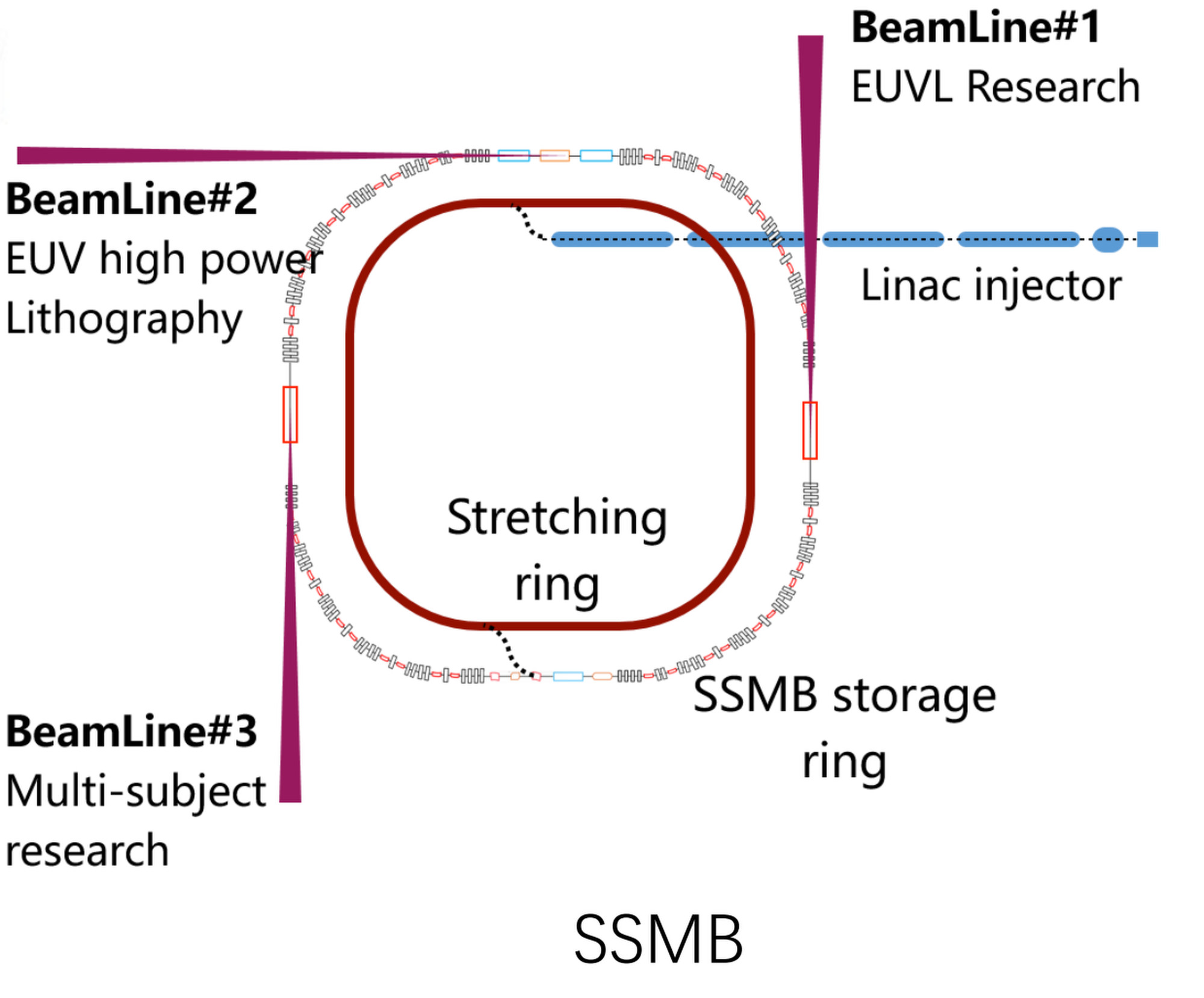
How the Tsinghua SSMB-EUV light source works. Photo: Tang Chuanxiang
Compared with current ASML EUV technology, SSMB is a more ideal light source. It has a higher average power and higher chip production output with lower unit cost.
ASML creates an EUV source from laser-produced plasma, where strong laser pulses are projected to liquid microdroplets of tin. The laser crushes the droplets and produces EUV pulse light during the impact. After complex filtering and focusing, an EUV light source with a power of about 250W is produced.
Before reaching the chip, the EUV beam undergoes reflection from 11 mirrors, each causing about a 30 per cent energy loss. As a result, the power of the beam is less than 5W when reaching the wafer. This can become an issue when manufacturing turns to 3nm or 2nm.
SSMB technology avoids such concerns. SSMB beams achieve a higher output power of 1000W, and due to its narrow bandwidth, fewer reflecting mirrors are needed, which naturally generates higher terminal power.
Zhao proposed this theory in 2010. Later, in 2017, Tang formed a dedicated team at Tsinghua.
The team conducted the first verification phase at Metrological Light Source (MLS) in Berlin, Germany. In 2019, the experiment was successful and they published a paper to illustrate the phenomenon in peer-reviewed journal Nature in 2021.
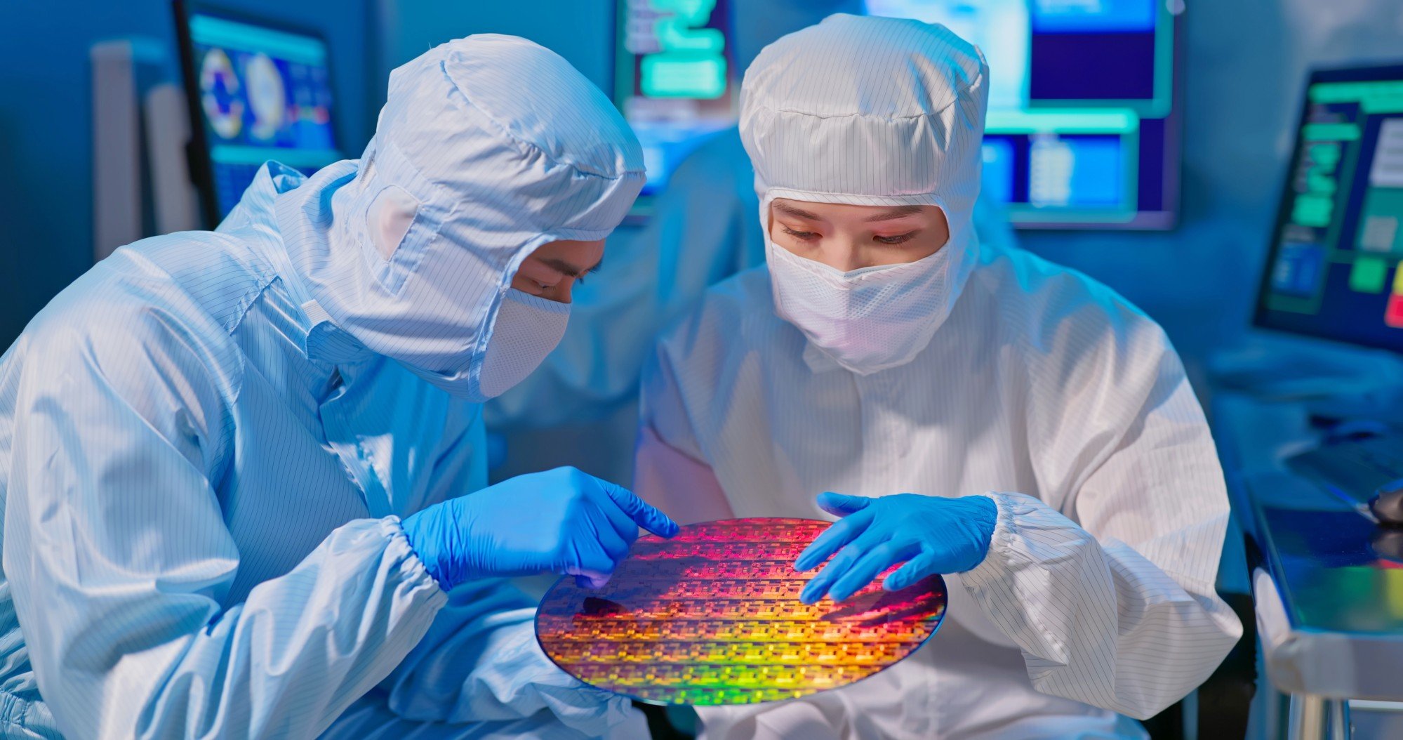
The new technology could see China become a global leader in microchip production. Photo: Shutterstock
Then in 2022, the team designed another prototype at Tsinghua University.
“An SSMB-EUV light source has been designed at THU, with designed EUV power higher than 1kW, and some key technologies are nearly ready,” said team member Professor Pan Zhilong during a presentation at an academic workshop in January 2022.
In February this year, the Hebei Provincial Science and Technology Department held a special meeting in Xiongan to discuss how to cultivate technology companies in the new district. Pan showed up to the meeting, further showcasing the team’s effort to bring SSMB to industry practice.
At the meeting, Pan introduced the plan for Tsinghua’s SSMB-EUV project. The team also visited Xiongan to select a site for future construction.
The establishment of a chip factory relies on funds and other engineering details. But more importantly, new ideas might bring new technical routes.
With no project progress disclosed to the public, Tang expected further efforts from the team and the industry to help SSMB grow.
“As a completely new light source, the experimental verification of the technology has been implemented. But it is necessary to build a solid SSMB light source research device operating in the EUV band,” Tang said in the Nature paper.
“Then we can [use the device to] cultivate scientific and industrial users, and polish the SSMB technology,” he said.
Tang believed the technology could help China get rid of future sanctions, but he did not talk about the specific progress of an SSMB-based lithography machine.
“There is still a long way to go before our independent development of EUV lithography machines, but SSMB-based EUV light sources give us an alternative to the sanctioned technology,” he said in the Tsinghua report.
“It requires continuous technological innovation based on SSMB EUV light sources and cooperation with upstream and downstream industries to build a usable lithography system.”
Tang also noted in the paper that the realisation of SSMB-EUV light sources will provide new tools for frontier research in materials science, basic physics, biochemistry and other disciplines.
China set to build giant chip factory using a particle accelerator
Unprecedented technology may offer a way to bypass US sanctions and see China lead semiconductor industry.