jamahir
ELITE MEMBER

- Joined
- Jul 9, 2014
- Messages
- 28,127
- Reaction score
- 1
- Country
- Location
The vacuum tube strikes back: NASA’s tiny 460GHz vacuum transistor that could one day replace silicon FETs

Way back in the salad days of digital computing (the 1940s and ’50s), computers were made of vacuum tubes — big, hot, clunky devices that, when you got right down to it, were essentially glorified light bulbs. This is why early computers like the ENIAC weighed more than 27 tons and consumed more power than a small town. Later, obviously, vacuum tubes would be replaced by probably the greatest invention of all time — the solid-state transistor — which would allow for the creation of smaller, faster, cheaper, and more reliable computers. Fast forward to 2014, though, and the humble CMOS field-effect transistor (FET) is starting to show its age. We’ve pretty much hit the limit on shrinking silicon transistors any further, and they can’t operate at speeds much faster than a few gigahertz. Which is why NASA’s Ames Research Center is going back to the future with its new vacuum transistor – a nanometer-scale vacuum tube that, in early testing, has reached speeds of up to 460GHz.
 The original vacuum tube triode, the main building block of early computers, consists of three separate elements inside a glass bulb. You have a cathode in the middle, which emits electrons; a grid around the cathode; and an anode around the outside. When a voltage is applied to the grid, electrons flow freely across the vacuum from the cathode to the anode. It is functionally identical to how a modern-day solid-state transistor works (a gate that controls the flow of electricity from source to drain). The main problem, though, was that the cathode had to be heated up by a filament so that it would emit electrons — and where there’s heat, there’s a lot of power consumption and a lot wear and tear. As you may know, it wasn’t unusual for old tube-based computers to break down every few hours whenever a tube burnt out.
So, anyway, the high running costs and frustrations of operating a tube-based computer were eventually assuaged by the discovery of processes that allowed for the cheap and plentiful production of integrated circuits with solid-state MOSFETs. And, in the last 40 years or so, we haven’t looked back. Until now.

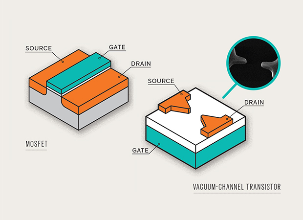
Standard MOSFET vs. vacuum-channel transistor [Image credit: IEEE Spectrum]
NASA’s Ames Research Center has been working on-and-off for many years on the vacuum-channel transistor, which is essentially a vacuum tube that can be fabricated using conventional CMOS techniques. Instead of a gate sitting between the source and drain, there is… nothing. A vacuum. By a method known as field emission, electrons are drawn across the vacuum from the source to the drain when a current is applied to the gate (see diagram). By using field emission rather than the thermionic (hot) electron emission, these vacuum-channel transistors don’t require a heat source. Importantly, they also don’t require a vacuum — instead they use helium (it’s sparse enough that the electrons have almost no chance of bumping into helium atoms while they traverse the few-nanometer gap between source and drain). The electrons also traverse the air gap a lot faster than if they had to pass through the gate electrode.

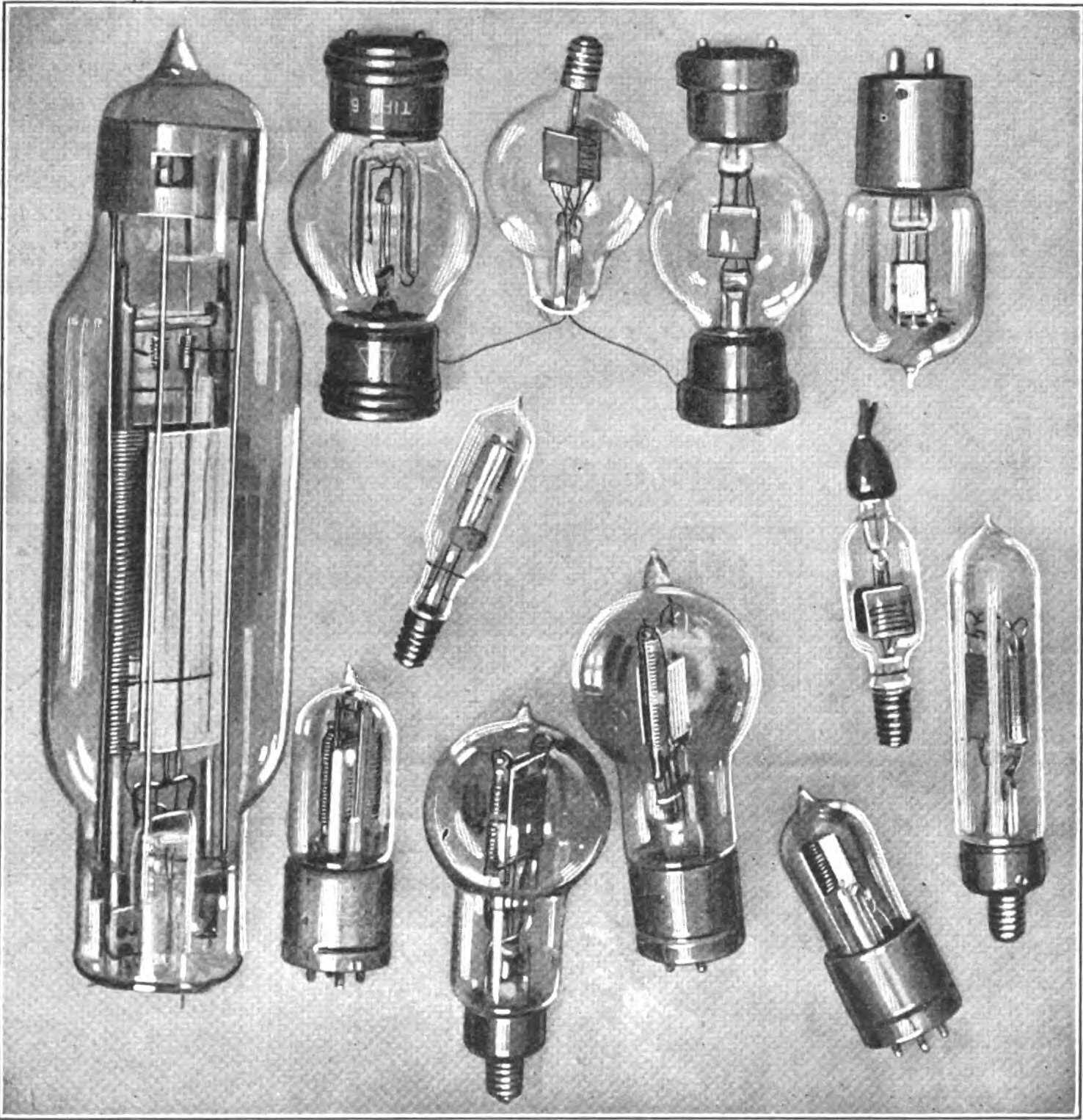
A collection of early triode vacuum tubes (Click to zoom in)
All in all, these vacuum-channel transistors, crazy as they sound, are surprisingly feasible. They can be fabricated using existing processes. The helium packaging is tougher, but the NASA researchers think that the techniques used to package current microelectromechanical sensors (gyroscopes, accelerometers) should be suitable for their unorthodox transistors as well. In early testing, a vacuum-channel transistor was able to operate at 460GHz — on the order of 10 times faster than a conventional, silicon-based FET (and comparable to the speeds that a graphene transistor might operate at). There’s no word on whether these vacuum-channel transistors will allow for the creation of small, modern audio amplifiers that sound like original tube amps — but maybe!
Moving forward, NASA is faced with the usual stumbling block that all new bleeding-edge technologies face: It’s built a single vacuum-channel transistor in the lab, and now it’s time to try and build large number of them on a single chip. The NASA researchers sound fairly positive about their chances — but really, until they actually get down to it, who knows what issues they might run into? In any case, add vacuum-channel transistors to the rather awesome (and rapidly growing) list of potential methods of pushing past the theoretical limits of silicon.
[Image credit: Kurt Faler]
--------------
source - The vacuum tube strikes back: NASA’s tiny 460GHz vacuum transistor that could one day replace silicon FETs | ExtremeTech
--------------
another, ( How vacuum tube technology is being deployed at the nanoscale ), from even earlier - october 2012...
--------------
@levina @thesolar65
- By Sebastian Anthony on June 24, 2014 at 8:12 am

Way back in the salad days of digital computing (the 1940s and ’50s), computers were made of vacuum tubes — big, hot, clunky devices that, when you got right down to it, were essentially glorified light bulbs. This is why early computers like the ENIAC weighed more than 27 tons and consumed more power than a small town. Later, obviously, vacuum tubes would be replaced by probably the greatest invention of all time — the solid-state transistor — which would allow for the creation of smaller, faster, cheaper, and more reliable computers. Fast forward to 2014, though, and the humble CMOS field-effect transistor (FET) is starting to show its age. We’ve pretty much hit the limit on shrinking silicon transistors any further, and they can’t operate at speeds much faster than a few gigahertz. Which is why NASA’s Ames Research Center is going back to the future with its new vacuum transistor – a nanometer-scale vacuum tube that, in early testing, has reached speeds of up to 460GHz.
 The original vacuum tube triode, the main building block of early computers, consists of three separate elements inside a glass bulb. You have a cathode in the middle, which emits electrons; a grid around the cathode; and an anode around the outside. When a voltage is applied to the grid, electrons flow freely across the vacuum from the cathode to the anode. It is functionally identical to how a modern-day solid-state transistor works (a gate that controls the flow of electricity from source to drain). The main problem, though, was that the cathode had to be heated up by a filament so that it would emit electrons — and where there’s heat, there’s a lot of power consumption and a lot wear and tear. As you may know, it wasn’t unusual for old tube-based computers to break down every few hours whenever a tube burnt out.
So, anyway, the high running costs and frustrations of operating a tube-based computer were eventually assuaged by the discovery of processes that allowed for the cheap and plentiful production of integrated circuits with solid-state MOSFETs. And, in the last 40 years or so, we haven’t looked back. Until now.

Standard MOSFET vs. vacuum-channel transistor [Image credit: IEEE Spectrum]
NASA’s Ames Research Center has been working on-and-off for many years on the vacuum-channel transistor, which is essentially a vacuum tube that can be fabricated using conventional CMOS techniques. Instead of a gate sitting between the source and drain, there is… nothing. A vacuum. By a method known as field emission, electrons are drawn across the vacuum from the source to the drain when a current is applied to the gate (see diagram). By using field emission rather than the thermionic (hot) electron emission, these vacuum-channel transistors don’t require a heat source. Importantly, they also don’t require a vacuum — instead they use helium (it’s sparse enough that the electrons have almost no chance of bumping into helium atoms while they traverse the few-nanometer gap between source and drain). The electrons also traverse the air gap a lot faster than if they had to pass through the gate electrode.

A collection of early triode vacuum tubes (Click to zoom in)
All in all, these vacuum-channel transistors, crazy as they sound, are surprisingly feasible. They can be fabricated using existing processes. The helium packaging is tougher, but the NASA researchers think that the techniques used to package current microelectromechanical sensors (gyroscopes, accelerometers) should be suitable for their unorthodox transistors as well. In early testing, a vacuum-channel transistor was able to operate at 460GHz — on the order of 10 times faster than a conventional, silicon-based FET (and comparable to the speeds that a graphene transistor might operate at). There’s no word on whether these vacuum-channel transistors will allow for the creation of small, modern audio amplifiers that sound like original tube amps — but maybe!
Moving forward, NASA is faced with the usual stumbling block that all new bleeding-edge technologies face: It’s built a single vacuum-channel transistor in the lab, and now it’s time to try and build large number of them on a single chip. The NASA researchers sound fairly positive about their chances — but really, until they actually get down to it, who knows what issues they might run into? In any case, add vacuum-channel transistors to the rather awesome (and rapidly growing) list of potential methods of pushing past the theoretical limits of silicon.
[Image credit: Kurt Faler]
--------------
source - The vacuum tube strikes back: NASA’s tiny 460GHz vacuum transistor that could one day replace silicon FETs | ExtremeTech
--------------
another, ( How vacuum tube technology is being deployed at the nanoscale ), from even earlier - october 2012...
"The thing is that vacuum tubes went away not because they were bad but because, with silicon, you could make everything so much smaller, and manufacture devices in the billions very cheaply," Meyyappan says.
"Actually, this was considered 20 years ago, when people tried to use microfabrication techniques and miniaturise vacuum tubes, but they did not perform that well," Meyyappan says.
Han's suggestion was that maybe it would be worth trying again, this time using the kind of nanoscale fabrication techniques that were not available two decades ago.
"Nanoscale vacuum tubes can provide high frequency and power output while satisfying the metrics of lightness, cost, lifetime, and stability at harsh conditions, and the operation voltage can be decreased comparable to modern semiconductor devices," the researchers say.
"Everything is done using silicon based technology – a conventional source and drain, standard optical lithography together with the technique of plasma ashing to create a nanogap separation of around 150nm between the emitter and collector," Meyyappan says. - See more at: How vacuum tube technology is being deployed at the nanoscale
People have talked about things like carbon nanotubes and graphene, but they just don't look like they are going to provide what we need – at least in the right time frame.
--------------
@levina @thesolar65


