The SC
ELITE MEMBER

- Joined
- Feb 13, 2012
- Messages
- 32,233
- Reaction score
- 21
- Country

- Location
GaN Technology for Radars
Keywords: GaN, gallium nitride, microwave devices, MMICs
Abstract
Microwave GaN technology is now in production and
poised to revolutionize many of today’s radar and
communication systems. Simultaneously, mm-wave GaN
processes are rapidly being matured to meet the growing
needs of high power and efficiency, at higher frequencies.
In this paper, we present an overview of GaN
development, focusing on reliability and affordability for
defense applications.
I
NTRODUCTION
His
torically, performance improvements afforded by new
microwave semiconductor technologies such as GaAs
MESFETs and PHEMTs have been evolutionary, resulting
in incrementally more power density, gain, or noise figure.
Gallium Nitride (GaN) technology, however, is truly
revolutionary, resulting in dramatic (>5X) improvements in
RF power density. The revolutionary power improvements
afforded by GaN are now being realized in state-of-the-art
monolithic
microwave integrated circuits (MMICs)
assembled in Transmit/Receive (T/R) modules, enabling the
next generation of radar and communication systems.
High power semiconductors play an important role in
radar performance. In a phased array radar, the RF energy is
distributed to each element, phase shifted and then amplified
before being radiated. The final amplification of the RF
signal at each element is performed by the power amplifier.
Traditionally, gallium arsenide (GaAs) has been the
semiconductor of choice for efficiently amplifying this
signal, creating the desired output power. Throughout the
1990’s, Raytheon and others pioneered the insertion of
GaAs-based MMICs into phased array radars, providing
enabling system capabilities. As the performance
requirements of these military systems have increased to
meet the ever growing threats, so too have the power and
efficiency requirements for the power amplifiers. Over that
time, GaAs performance was stretched from the unit gate
power density of 0.5 watt per millimeter of transistor
periphery to 1.5 W/mm by increasing the drain voltage from
5V to nearly 24V. GaN, however, continued to make
dramatic performance and maturity improvements, quickly
surpassing GaAs’ capability in power, efficiency, thermal
spreading, cost effectiveness and frequency coverage
(Table 1).
Today, with the development of microwave GaN
complete, the power, efficiency and bandwidth performance
of GaN-based MMICs is unsurpassed, revolutionizing the
design of radars by creating not only higher performance but
also lower system cost. With over 5 W/mm of power
density, GaN RF amplifiers can provide more than 5X the
power per element of GaAs, in the same square millimeter
area footprint. Fewer high power GaN MMICs can be used
to replace many low power GaAs MMICs, or alternatively,
equal power GaN chips can be made dramatically smaller
than their GaAs equivalent. Both approaches reduce overall
system costs while enabling size-constrained systems. The
higher drain current that GaN offers makes the broadband
matching of high power MMICs simpler and more efficient
than GaAs, while the 7-8X improvement in the thermal
conductivity provided by the high conductivity SiC substrate
enables amplifier cooling. This higher efficiency, achieved
at high power, combined with better thermal dissipation, is a
game changer for solid state electronic warfare systems.
Finally, the wide band gap intrinsic to GaN material
provides large critical breakdown fields and voltages,
making a more robust amplifier, which eases T/R module
and system implementation.
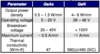
Table 1. GaN vs. GaAs Comparison
Parameter
GaAs
GaN
Output power
density
0.5 – 1.5 W/mm
4– 8 W/mm
Operating voltage
5 – 20 V
28 – 48 V
Breakdown
voltage
20 – 40V
> 100V
Maximum current
~ 0.5 A/mm
~1 A/mm
Thermal
conductivity
(W/m-K)
47
390(z)/490 (SiC)
This paper will review the advances in GaN device
development, starting in the 1990’s with the first transistor
to its production status today. DC Arrhenius reliability data
CS MANTECH Conference, April 23rd - 26th, 2012, Boston, Massachusetts, USA
and RF operating life measurements of Raytheon’s
microwave process will also be presented. Finally, sample
MMIC designs will be reviewed, along with system insertion
considerations, including cost and thermal constraints.
G
A
N
D
EVELOPMENT
The development of GaN semiconductors began more
than 30 years ago, driven by their unique properties
seemingly ideal for high-power microwave devices based on
their high theoretical breakdown field and high saturated
electron velocity. But at that time, the gallium nitride
material quality was insufficient to produce microwave RF
transistors. This all began to change in the early 1990s,
Figure 1, when researchers used gallium nitride to fabricate
the world’s first green, blue, violet and white light-emitting
diodes (LEDs) [1,2]. This breakthrough drove forward a
rapid improvement in GaN material quality. Now, these
LEDs can be found in traffic lights, TVs and flashlights.
Another obstacle to the development of GaN transistors
was the lack of an inexpensive substrate material.
Traditionally, the substrate material of the transistor is the
same material as the transistor itself, but, to date, researchers
have been unable to grow large area, high quality GaN
substrates. Researchers first turned to growing GaN
transistors on sapphire substrates, and in 1996 demonstrated
the first microwave GaN power transistors. The sapphire
substrates are low cost and widely available; however, their
poor thermal conductivity and non-ideal lattice match to
GaN limited the performance of the transistors. Semi-
insulating silicon carbide (SiC) substrate proved a better
choice with a good lattice match to GaN and an excellent
thermal conductivity. The only drawback was that silicon
carbide substrates were only available in small sizes (50 mm
diameter) and were very expensive (100 times the price of
GaAs) in the late 1990s. The last 10 years have seen a rapid
improvement in the size, quality and cost of the silicon
carbide substrates. Today, Raytheon’s production GaN
process uses 100 mm (4-inch) diameter SiC substrates [3,4].
Figure 1. Timeline of GaN development
R
ELIABILITY
Over the last six years, through the testing of hundreds of
transistors and MMICs, Raytheon’s 4” microwave GaN
processes has demonstrated the required reliability for
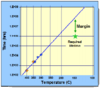
military systems. Figure 2 shows the DC Arrhenius results
of a population of ~70 devices tested at five highly
accelerated temperatures and 28V bias. The activation
energy is ~1.7eV with a median time to failure (MTTF) at
150C of ~10
8
hours [5], exceeding the 10
6
hr standard.
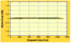
Figure 3 shows no change in output power of twelve X-band
MMICs operating ~3-4 dB compressed at 28V for more than
1,000 hours. Channel temperatures are estimated to be
~150C-200C during this RF operating test. Additional
testing for more than 15,000 hours on X-band MMICs has
yielded similar results.
Figure 2. DC Arrhenius results of accelerated testing of
10x125um GaN transistors operating at 28V.
-2
-1.5
-1
-0.5
0
0.5
1
1.5
2
0
200
400
600
800
1000
1200
Delta Pout (dB)
Elapsed time (hrs)
Figure 3. A dozen X-band MMICs demonstrating no change
in output power over 1,000 hrs of RF operation at 28V.
MMIC
S
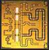
Raytheon has developed MMICs using both microstrip
and coplanar waveguide (CPW) circuit design techniques,
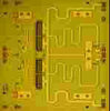
each of which offers advantages. Figure 4 shows two low
frequency MMICs designed and fabricated using both
topologies, and which demonstrated similar performance and
size. The CPW process is lower in cost and higher yielding
since it eliminates the backside grinding and via process, but
at higher frequencies the output matching network becomes
CS MANTECH Conference, April 23rd - 26th, 2012, Boston, Massachusetts, USA
higher loss using this technique. In a face-up module
implementation, the CPW design also offers a superior
conduction path due the heat spreading of the thick SiC
material. The microstrip MMIC offers slightly lower loss
and is easier to design, allowing for faster design iterations.
Figure 4. Fabricated low frequency Microstrip (left) and
CPW (right) GaN MMICs
With the maturation of GaN in the lower RF frequency
operating range, development focus has now shifted to GaN
at mm-wave frequencies. At the extreme of the mm-wave
RF frequency band, we have fabricated a 3-stage W-band
GaN MMIC using a 2mil thick, microstrip topology
operating at 17V [6]. This compact MMIC is less than
2.5mm
2
and has 16 dB of small signal gain at 91 GHz.
Un
der large signal compressed operation, the MMIC
delivered 1.2W of output power and 20% PAE. These
results compare favorably to the best efficiency
demonstrated at this frequency using high gain, lower power
InP technology, but at many multiples of output power.
S
YSTEM
I
NSERTIONS
G
aN offers a number of advantages for next generation
radars and jammers, as well as upgrades to existing GaAs or
tube-based systems. Fewer high power GaN MMICs can be
used to replace either many low power GaAs
MMICs/modules or a single, often unreliable, high power
tube, reducing overall cost while improving system
reliability. For a fixed power level, a GaN MMIC can be
1/3-1/4 the size of an equivalent power GaAs MMIC due to
the higher power density transistors. While the GaN
starting material (GaN on SiC) is considerably more
expensive than GaAs, the reduced area to generate similar
power allows the GaN solution to be less expensive. For
example, if the finished GaN wafer (including material)
costs 2X that of GaAs, but yet the GaN MMIC is 1/3-1/4 the
size of the GaAs MMIC, the resulting GaN solution is only
50-66% the dollars per RF Watt generated. A GaN-based
system also provides additional benefits over GaAs at the
system level by reducing overall module count, a major
system cost driver, and the higher operating voltage
improves the DC to RF conversion efficiency, reducing
prime power and life cycle costs. For systems where
maximum power per unit cell is desired, GaN offers ~5X
power improvement in the same mm
2
as GaAs, enabling
ma
ny space-constrained systems.
C
ONCLUSIONS
G
aN material, processing, MMIC design and system
insertion has matured greatly over the last decade, driven by
its ability to increase the capability of RF systems, while
reducing their cost. Today, GaN is quickly becoming the
power amplification standard for all RF systems and is being
assembled into modules and radars (Figure 5).
http://csmantech.pairserver.com/newsite/gaasmantech/Digests/2012/papers/3.2.011.pdf
Keywords: GaN, gallium nitride, microwave devices, MMICs
Abstract
Microwave GaN technology is now in production and
poised to revolutionize many of today’s radar and
communication systems. Simultaneously, mm-wave GaN
processes are rapidly being matured to meet the growing
needs of high power and efficiency, at higher frequencies.
In this paper, we present an overview of GaN
development, focusing on reliability and affordability for
defense applications.
I
NTRODUCTION
His
torically, performance improvements afforded by new
microwave semiconductor technologies such as GaAs
MESFETs and PHEMTs have been evolutionary, resulting
in incrementally more power density, gain, or noise figure.
Gallium Nitride (GaN) technology, however, is truly
revolutionary, resulting in dramatic (>5X) improvements in
RF power density. The revolutionary power improvements
afforded by GaN are now being realized in state-of-the-art
monolithic
microwave integrated circuits (MMICs)
assembled in Transmit/Receive (T/R) modules, enabling the
next generation of radar and communication systems.
High power semiconductors play an important role in
radar performance. In a phased array radar, the RF energy is
distributed to each element, phase shifted and then amplified
before being radiated. The final amplification of the RF
signal at each element is performed by the power amplifier.
Traditionally, gallium arsenide (GaAs) has been the
semiconductor of choice for efficiently amplifying this
signal, creating the desired output power. Throughout the
1990’s, Raytheon and others pioneered the insertion of
GaAs-based MMICs into phased array radars, providing
enabling system capabilities. As the performance
requirements of these military systems have increased to
meet the ever growing threats, so too have the power and
efficiency requirements for the power amplifiers. Over that
time, GaAs performance was stretched from the unit gate
power density of 0.5 watt per millimeter of transistor
periphery to 1.5 W/mm by increasing the drain voltage from
5V to nearly 24V. GaN, however, continued to make
dramatic performance and maturity improvements, quickly
surpassing GaAs’ capability in power, efficiency, thermal
spreading, cost effectiveness and frequency coverage
(Table 1).
Today, with the development of microwave GaN
complete, the power, efficiency and bandwidth performance
of GaN-based MMICs is unsurpassed, revolutionizing the
design of radars by creating not only higher performance but
also lower system cost. With over 5 W/mm of power
density, GaN RF amplifiers can provide more than 5X the
power per element of GaAs, in the same square millimeter
area footprint. Fewer high power GaN MMICs can be used
to replace many low power GaAs MMICs, or alternatively,
equal power GaN chips can be made dramatically smaller
than their GaAs equivalent. Both approaches reduce overall
system costs while enabling size-constrained systems. The
higher drain current that GaN offers makes the broadband
matching of high power MMICs simpler and more efficient
than GaAs, while the 7-8X improvement in the thermal
conductivity provided by the high conductivity SiC substrate
enables amplifier cooling. This higher efficiency, achieved
at high power, combined with better thermal dissipation, is a
game changer for solid state electronic warfare systems.
Finally, the wide band gap intrinsic to GaN material
provides large critical breakdown fields and voltages,
making a more robust amplifier, which eases T/R module
and system implementation.
Table 1. GaN vs. GaAs Comparison
Parameter
GaAs
GaN
Output power
density
0.5 – 1.5 W/mm
4– 8 W/mm
Operating voltage
5 – 20 V
28 – 48 V
Breakdown
voltage
20 – 40V
> 100V
Maximum current
~ 0.5 A/mm
~1 A/mm
Thermal
conductivity
(W/m-K)
47
390(z)/490 (SiC)
This paper will review the advances in GaN device
development, starting in the 1990’s with the first transistor
to its production status today. DC Arrhenius reliability data
CS MANTECH Conference, April 23rd - 26th, 2012, Boston, Massachusetts, USA
and RF operating life measurements of Raytheon’s
microwave process will also be presented. Finally, sample
MMIC designs will be reviewed, along with system insertion
considerations, including cost and thermal constraints.
G
A
N
D
EVELOPMENT
The development of GaN semiconductors began more
than 30 years ago, driven by their unique properties
seemingly ideal for high-power microwave devices based on
their high theoretical breakdown field and high saturated
electron velocity. But at that time, the gallium nitride
material quality was insufficient to produce microwave RF
transistors. This all began to change in the early 1990s,
Figure 1, when researchers used gallium nitride to fabricate
the world’s first green, blue, violet and white light-emitting
diodes (LEDs) [1,2]. This breakthrough drove forward a
rapid improvement in GaN material quality. Now, these
LEDs can be found in traffic lights, TVs and flashlights.
Another obstacle to the development of GaN transistors
was the lack of an inexpensive substrate material.
Traditionally, the substrate material of the transistor is the
same material as the transistor itself, but, to date, researchers
have been unable to grow large area, high quality GaN
substrates. Researchers first turned to growing GaN
transistors on sapphire substrates, and in 1996 demonstrated
the first microwave GaN power transistors. The sapphire
substrates are low cost and widely available; however, their
poor thermal conductivity and non-ideal lattice match to
GaN limited the performance of the transistors. Semi-
insulating silicon carbide (SiC) substrate proved a better
choice with a good lattice match to GaN and an excellent
thermal conductivity. The only drawback was that silicon
carbide substrates were only available in small sizes (50 mm
diameter) and were very expensive (100 times the price of
GaAs) in the late 1990s. The last 10 years have seen a rapid
improvement in the size, quality and cost of the silicon
carbide substrates. Today, Raytheon’s production GaN
process uses 100 mm (4-inch) diameter SiC substrates [3,4].
Figure 1. Timeline of GaN development
R
ELIABILITY
Over the last six years, through the testing of hundreds of
transistors and MMICs, Raytheon’s 4” microwave GaN
processes has demonstrated the required reliability for
military systems. Figure 2 shows the DC Arrhenius results
of a population of ~70 devices tested at five highly
accelerated temperatures and 28V bias. The activation
energy is ~1.7eV with a median time to failure (MTTF) at
150C of ~10
8
hours [5], exceeding the 10
6
hr standard.
Figure 3 shows no change in output power of twelve X-band
MMICs operating ~3-4 dB compressed at 28V for more than
1,000 hours. Channel temperatures are estimated to be
~150C-200C during this RF operating test. Additional
testing for more than 15,000 hours on X-band MMICs has
yielded similar results.
Figure 2. DC Arrhenius results of accelerated testing of
10x125um GaN transistors operating at 28V.
-2
-1.5
-1
-0.5
0
0.5
1
1.5
2
0
200
400
600
800
1000
1200
Delta Pout (dB)
Elapsed time (hrs)
Figure 3. A dozen X-band MMICs demonstrating no change
in output power over 1,000 hrs of RF operation at 28V.
MMIC
S
Raytheon has developed MMICs using both microstrip
and coplanar waveguide (CPW) circuit design techniques,
each of which offers advantages. Figure 4 shows two low
frequency MMICs designed and fabricated using both
topologies, and which demonstrated similar performance and
size. The CPW process is lower in cost and higher yielding
since it eliminates the backside grinding and via process, but
at higher frequencies the output matching network becomes
CS MANTECH Conference, April 23rd - 26th, 2012, Boston, Massachusetts, USA
higher loss using this technique. In a face-up module
implementation, the CPW design also offers a superior
conduction path due the heat spreading of the thick SiC
material. The microstrip MMIC offers slightly lower loss
and is easier to design, allowing for faster design iterations.
Figure 4. Fabricated low frequency Microstrip (left) and
CPW (right) GaN MMICs
With the maturation of GaN in the lower RF frequency
operating range, development focus has now shifted to GaN
at mm-wave frequencies. At the extreme of the mm-wave
RF frequency band, we have fabricated a 3-stage W-band
GaN MMIC using a 2mil thick, microstrip topology
operating at 17V [6]. This compact MMIC is less than
2.5mm
2
and has 16 dB of small signal gain at 91 GHz.
Un
der large signal compressed operation, the MMIC
delivered 1.2W of output power and 20% PAE. These
results compare favorably to the best efficiency
demonstrated at this frequency using high gain, lower power
InP technology, but at many multiples of output power.
S
YSTEM
I
NSERTIONS
G
aN offers a number of advantages for next generation
radars and jammers, as well as upgrades to existing GaAs or
tube-based systems. Fewer high power GaN MMICs can be
used to replace either many low power GaAs
MMICs/modules or a single, often unreliable, high power
tube, reducing overall cost while improving system
reliability. For a fixed power level, a GaN MMIC can be
1/3-1/4 the size of an equivalent power GaAs MMIC due to
the higher power density transistors. While the GaN
starting material (GaN on SiC) is considerably more
expensive than GaAs, the reduced area to generate similar
power allows the GaN solution to be less expensive. For
example, if the finished GaN wafer (including material)
costs 2X that of GaAs, but yet the GaN MMIC is 1/3-1/4 the
size of the GaAs MMIC, the resulting GaN solution is only
50-66% the dollars per RF Watt generated. A GaN-based
system also provides additional benefits over GaAs at the
system level by reducing overall module count, a major
system cost driver, and the higher operating voltage
improves the DC to RF conversion efficiency, reducing
prime power and life cycle costs. For systems where
maximum power per unit cell is desired, GaN offers ~5X
power improvement in the same mm
2
as GaAs, enabling
ma
ny space-constrained systems.
C
ONCLUSIONS
G
aN material, processing, MMIC design and system
insertion has matured greatly over the last decade, driven by
its ability to increase the capability of RF systems, while
reducing their cost. Today, GaN is quickly becoming the
power amplification standard for all RF systems and is being
assembled into modules and radars (Figure 5).
http://csmantech.pairserver.com/newsite/gaasmantech/Digests/2012/papers/3.2.011.pdf