What's new

Huawei EUV Scanner Patent Suggests Sub-7nm Chips for China

onebyone

SENIOR MEMBER
Joined
Jul 2, 2014
Messages
7,550
Reaction score
-6
Country
Thailand
Location
Thailand

Huawei EUV Scanner Patent Suggests Sub-7nm Chips for China​

By Anton Shilov
published about 19 hours ago
Huawei files a patent application covering EUV scanners.
MonXfTxS6dUdakg6EQGPcQ-320-80.jpg

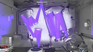
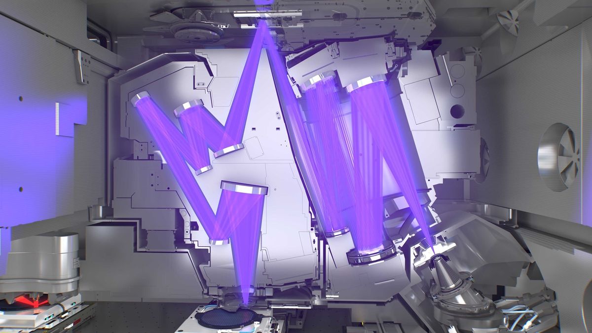
(Image credit: ASML)

Huawei has filed a patent application covering an extreme ultraviolet (EUV) lithography scanner, according to UDN. If the company builds such a scanner and achieves decent productivity, uptime, and yields, Chinese chipmakers could produce chips on sub-7nm-class technologies. The only question is when.

In mid-November, Huawei filed an application with the State Intellectual Property Office for a patent covering an EUV scanner and its key components. The patent application number is 202110524685X, reports MyDrivers.
The patent application appears to cover all crucial components of an EUV scanner, including a 13.5 nm EUV light generator (light source), a set of reflecting mirrors, the lithography system, and 'control management technologies' (we would speculate that this is how they call metrology), according to descriptions published by various media sources.

Filing a patent is not equal to being able to build an EUV scanner, which is a highly complex machine featuring numerous state-of-the-art components that have to work perfectly in concert and for prolonged amounts of time. Furthermore, even with an EUV tool at hand, chipmakers still have to figure out the right pellicles for masks, resists, and many other things necessary for high-volume production.
missing-image.svg

An EUV scanner with a 0.33 numerical aperture is the pinnacle of today's semiconductor production tools. Numerous companies attempted to develop such a tool, but only ASML succeeded after over ten years of development and with financial support from Intel, Samsung, and TSMC. Today, Samsung, SK Hynix, and TSMC actively use EUV tools from ASML, but Intel has yet to start high-volume chip production using these tools.


For now, only Intel, Micron, Samsung, SK Hynix, and TSMC either use or plan to use EUV scanners. Moreover, only these five companies have developed (or plan to develop) process technologies sophisticated enough to take advantage of EUV scanners. Meanwhile, China-based SMIC could not get an already procured EUV tool to develop its own EUV-based fabrication process due to the Wassenaar arrangement. Therefore, it is evident that demand for EUV scanners potentially exists in China, and apparently, Huawei was eager to address it.

As a world-class high-tech conglomerate with some $100 billion in annual revenue, Huawei pursues different goals and develops many technologies. The company's semiconductor production ambitions are well known, and they are not limited to chip production but also to building wafer fab equipment. Huawei's WFE efforts are advancing pretty well as the company applied for a patent covering an EUV scanner.
 
Huawei confirms breakthrough in EUV lithography process optimization :yahoo:

Judy Lin, DIGITIMES Asia, Taipei
Monday 26 December 20220

1_b.jpg

Credit: DIGITIMES

Huawei has confirmed in a posting on its website reports about its breakthrough in making a light source component used in EUV lithography systems which are required for making high-end processors on sub-10 nm nodes. :enjoy:

The Chinese tech giant posted a video on its website to back claims about its EUV lithography breakthrough. It also claimed to have "entered the game" on its official website.

China tech news media MyDrivers quoted China's National Intellectual Properties Administration website information saying that Huawei Technology filed an application for a patent covering a EUV lithography process and its key components in mid-November. The patent application number is 202110524685X.

Huawei's application has not been approved yet. It is difficult to judge whether Huawei already has the ability to produce the entire EUV equipment.
Huawei said on its website the latest patent application shows the usage of EUV lithography technology to improve the manufacturing of integrated is circuits and chipsets.

"Together, this process will form an interference pattern that will keep on changing with new light rays.

Consequently, this will equalize the light exposure and will solve the un-uniform light issues that often occur in chip development," according to Huawei's website description.

Alongside uniform light rays, this mechanism will ease the creation and formation of the nano-particles that are assembled in the integrated circuits or the micro-chipsets.

"Further, lithography mainly performs the transfer, processing, and creation of micro-nano graphics. It also verifies the total elements equipped in a chipset and checks the appropriate size and other details in the circuits," according to Huawei.

A UDN report said in addition to Huawei, local research institutions in China, such as Tsinghua, have also put forward EUV lithography-related technologies to overcome the light source technology barriers, mastering new light sources that can be used for EUV lithography. The Chinese Academy of Sciences also mastered the mirror system technology.

Despite the breakthrough in EUV light source technology, the EUV machine is not easy to manufacture, because there are more than 100,000 components in a EUV machine, requiring the collaboration of a huge supply chain, which is a major obstacle for any country trying to build the equipment from scratch without getting help from other component sources.

Huawei has been quietly developing a domestic semiconductor ecosystem over the past few years trying to counter the US tech export sanctions that have kept it from accessing advanced chips. It has invested in a wide range of companies in the semiconductor supply chain, starting from EDA, equipment, and materials, to foundry, testing, and packaging.

The technology for which Huawei is applying for a patent is trying to solve the problem of uneven light intensity of the light source used in the EUV lithography machine. According to the disclosed information, the patent application provides a reflector, a lithography device, and a control method thereof, which relates to the field of optics and can solve the problem that coherent light cannot be homogenized due to the formation of a fixed interference pattern and is optimized on the basis of the lithography device for extreme ultraviolet light, thus achieving the purpose of homogenization.

:o: The UDN report said while Huawei is developing EUV lithography, it is also developing technologies that "bypass" lithography. :o:. For example, it is bypassing the US monopoly technology of silicon wafers in favor of optoelectronic wafers and other practices.

Interestingly, ASML, the company which is the sole provider of EUV equipment in the world, applied for a similar patent (US2016007434A1) in 2016 but has a different scope of patent rights.

The difference between the two patents is that Huawei uses a rotating illumination device to reduce the number of bright or dark patterns in the same area, while ASML's patent allows the same beam of light to be split and incident at different points to produce a uniform light on the relative movable and stationary flat panels and reflector sets.

ASML's EUV machine uses Cymer's light source device. Cymer is headquartered in San Diego, California, and was acquired by ASML in 2013.

It took ASML 17 years to develop the first-generation multi-patterning EUV equipment, which has been used only by TSMC, Samsung, Micron, Intel, and SK Hynix so far. Currently, China is prohibited from accessing EUVs, but is able to import DUVs which are used to produce mature node chips of 28nm and above.

According to ASML's website, its EUV technology uses light with a wavelength of 13.5nm, which is more than 14 times shorter than DUV light.
The laser-produced plasma (LPP) source, molten tin droplets of around 25 microns in diameter are ejected from a generator at 70 meters per second. As they fall, the droplets are hit first by a low-intensity laser pulse that flattens them into a pancake shape. Then a more powerful laser pulse vaporizes the flattened droplet to create a plasma that emits EUV light.

To produce enough light to manufacture microchips, this process is repeated 50,000 times every second.
ASML has announced in its third-quarter 2022 earnings conference call that it will continue to ship DUV lithography equipment to China and that it will increase its production capacity to 90 EUV and 600 DUV systems (2025-2026) and increase its High-NA EUV capacity to 20 systems (2027-2028).


I am reading lots of PHD papers to get a feeling of China's EUVL advance. The most important component of ASML is laser source, which is supplied by US Cymer and lens, which is supplied by German Zeiss.

ASML is just a system integrator.

On some individual component, China is very close to world class. China seems to be able to produce high power 13.5nm laser reliably. Earlier I predict China indigenous EUL machine to come on line 2040. Now I am a little more optimistic.

We may see a China EUVL prototype 2030.

I also suspect there is a serious stagnation in western technologies. Over the years, the western elites being fearful of smart people, promotes diverisity and MBA, putting the most stupid and evil people in charge. Soon there will be a gradual death of a lot of white man high tech,

Right now Huawei is at the patent level. I think there are still a few years to go. I think that's why the older chip production has been increased utilizing 28nm chips. But it would be interesting to see how quickly can China roll out <13nm chips en masses. There is still the manufacturing, labor training processes that need to be established and just meeting local demand would be a hassle. Then comes deployment to international markets.
 
The dumb Yanks awakened the sleeping giant by sanctioning this and that. Nothing motivates China than sanctions. It unites all of Chinese society towards one goal and accelerates domestic development.
 
The dumb Yanks awakened the sleeping giant by sanctioning this and that. Nothing motivates China than sanctions. It unites all of Chinese society towards one goal and accelerates domestic development.

That's right. China stands for justice. Huns bullied Chinese and see what happened to them. Same will happen with Anglos.
 

Back
Top Bottom