The SC
ELITE MEMBER

- Joined
- Feb 13, 2012
- Messages
- 32,233
- Reaction score
- 21
- Country

- Location
(Nanowerk News) Nanotechnology is regarded as the key technology of the 21st century, delivering the fundamental methods, which allow objects just a few hundred nanometers in size to be produced in any required shape. These objects find applications practically everywhere – be it for microprocessors and electrical circuits in computers, in the telecommunications industry, or in medicine and biotechnology – to name just a few.
To encourage the development of new manufacturing processes the EU recently established the Marie Curie Training Network ELENA (low energy electron-driven chemistry for the advantage of emerging nanofabrication methods). Empa is one of the project partners, together with 13 universities, three research institutes and five industrial partners, drawn from a total of 13 countries.
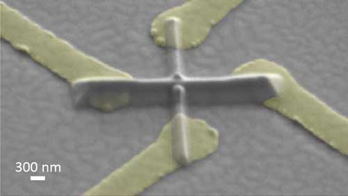
A magnetic sensor additively written with a focused electron beam and Co2(CO)8 molecules, located between four previously-structured gold electrodes. The sensor can be given any required shape by moving the substrate or adjusting the dwell time of the electron beam.
The aim of this large-scale project is to provide training for young European scientists in the field of nanotechnology so that they can generate the innovative ideas necessary to further research and scientific exploitation, so enhancing Europe’s international competitivity. The network is led by Oddur Ingólfsson of the Icelandic University in Reykjavík, Empa’s representative is Ivo Utke from the Mechanics of Materials and Nanostructures laboratory in Thun.
Empa was already involved in the predecessor project to "ELENA", the COST-Action Network "CELINA" (chemistry for electron-induced nanofabrication), where it worked closely with some of the universities now participating in the current project. The aim of "CELINA" was to investigate the suitability of low volatility materials for directly writing with focused electron beams using a gas injection system (developed in-house) with a scanning electron microscope.
Over the coming four years the EU will make available about €4 million for ELENA. Two state-of-the-art nanotechnology processes are the focus of the network: Focused Electron Beam Induced Deposition, (FEBID) and Extreme Ultraviolet Lithography (EUVL).
Writing extremely fine structures in three dimensions
The FEBID technique makes use of an extremely finely focused electron beam. This is used to “write” three-dimensional structures of any required shape on a surface, such as the silicon wafers from which computer chips are manufactured.
The structures are created by a form of "Additive Manufacturing", in that absorbing molecules, which are continuously supplied to the surface in question, are then broken up by an electron beam, following which certain parts of the molecule are locally deposited onto the substrate. The process requires the use of molecules containing the necessary component parts – these are then freed by the electron beam to create the required material composition on the substrate.
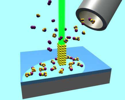
FEBID: within a scanning electron microscope molecules supplied continuously to a point on the surface are locally decomposed by a focused electron beam. This creates an "Additive Manufacturing" platform with a lateral resolution of less than 10 nm. Empa researchers are investigating how to control the decomposition products.
Imprinting functional materials
In the course of the ELENA project material scientists, chemists and physicists will work together to develop and test molecules which are suitable for the FEBID technique. This process has been the subject of research at Empa for the past 10 years or so and has already been successfully applied to writing magnetic sensors with the highest lateral magnetic resolution.
For this purpose the Empa researchers used the Co2(CO)8 molecule, which allowed them to write a granular cobalt compound with special magnetic properties in a carbon-containing matrix on a silicon oxide layer between several gold electrodes. Another application has been realised in the area of nanophotonics: the initial substance, gold Me2Au(tfa) was used to write an optical lattice on a vertically-cavity surface emitting laser in a minimally invasive manner.
The EUVL technique also imprints extremely fine structures on surfaces, although it is limited to two dimensions. Specially adapted materials are also necessary for this process to function correctly, in this case thin films known as photoresists. When these films are irradiated with EUV light in the appropriate way they efficiently and precisely create the required structures.
The search for new molecules for additive writing on pure metals using FEBID, and new photoresists for EUVL is at the focus of the research efforts of a total of 15 outstanding doctoral students working on the ELENA project. Ivo Utke’s group, with two postdocs and three PhD students, is testing possible ways of controlling the deposited components of the absorbing molecule as a function of the intensity of the electron beams and molecule flows in a scanning electron microscope.
http://www.nanowerk.com/nanotechnology-news/newsid=45599.php
To encourage the development of new manufacturing processes the EU recently established the Marie Curie Training Network ELENA (low energy electron-driven chemistry for the advantage of emerging nanofabrication methods). Empa is one of the project partners, together with 13 universities, three research institutes and five industrial partners, drawn from a total of 13 countries.
A magnetic sensor additively written with a focused electron beam and Co2(CO)8 molecules, located between four previously-structured gold electrodes. The sensor can be given any required shape by moving the substrate or adjusting the dwell time of the electron beam.
The aim of this large-scale project is to provide training for young European scientists in the field of nanotechnology so that they can generate the innovative ideas necessary to further research and scientific exploitation, so enhancing Europe’s international competitivity. The network is led by Oddur Ingólfsson of the Icelandic University in Reykjavík, Empa’s representative is Ivo Utke from the Mechanics of Materials and Nanostructures laboratory in Thun.
Empa was already involved in the predecessor project to "ELENA", the COST-Action Network "CELINA" (chemistry for electron-induced nanofabrication), where it worked closely with some of the universities now participating in the current project. The aim of "CELINA" was to investigate the suitability of low volatility materials for directly writing with focused electron beams using a gas injection system (developed in-house) with a scanning electron microscope.
Over the coming four years the EU will make available about €4 million for ELENA. Two state-of-the-art nanotechnology processes are the focus of the network: Focused Electron Beam Induced Deposition, (FEBID) and Extreme Ultraviolet Lithography (EUVL).
Writing extremely fine structures in three dimensions
The FEBID technique makes use of an extremely finely focused electron beam. This is used to “write” three-dimensional structures of any required shape on a surface, such as the silicon wafers from which computer chips are manufactured.
The structures are created by a form of "Additive Manufacturing", in that absorbing molecules, which are continuously supplied to the surface in question, are then broken up by an electron beam, following which certain parts of the molecule are locally deposited onto the substrate. The process requires the use of molecules containing the necessary component parts – these are then freed by the electron beam to create the required material composition on the substrate.
FEBID: within a scanning electron microscope molecules supplied continuously to a point on the surface are locally decomposed by a focused electron beam. This creates an "Additive Manufacturing" platform with a lateral resolution of less than 10 nm. Empa researchers are investigating how to control the decomposition products.
Imprinting functional materials
In the course of the ELENA project material scientists, chemists and physicists will work together to develop and test molecules which are suitable for the FEBID technique. This process has been the subject of research at Empa for the past 10 years or so and has already been successfully applied to writing magnetic sensors with the highest lateral magnetic resolution.
For this purpose the Empa researchers used the Co2(CO)8 molecule, which allowed them to write a granular cobalt compound with special magnetic properties in a carbon-containing matrix on a silicon oxide layer between several gold electrodes. Another application has been realised in the area of nanophotonics: the initial substance, gold Me2Au(tfa) was used to write an optical lattice on a vertically-cavity surface emitting laser in a minimally invasive manner.
The EUVL technique also imprints extremely fine structures on surfaces, although it is limited to two dimensions. Specially adapted materials are also necessary for this process to function correctly, in this case thin films known as photoresists. When these films are irradiated with EUV light in the appropriate way they efficiently and precisely create the required structures.
The search for new molecules for additive writing on pure metals using FEBID, and new photoresists for EUVL is at the focus of the research efforts of a total of 15 outstanding doctoral students working on the ELENA project. Ivo Utke’s group, with two postdocs and three PhD students, is testing possible ways of controlling the deposited components of the absorbing molecule as a function of the intensity of the electron beams and molecule flows in a scanning electron microscope.
http://www.nanowerk.com/nanotechnology-news/newsid=45599.php